- 您现在的位置:买卖IC网 > Sheet目录39246 > LM2685MTCX/NOPB (NATIONAL SEMICONDUCTOR CORP) SWITCHED CAPACITOR REGULATOR, 180 kHz SWITCHING FREQ-MAX, PDSO14
Detailed Device Description
The LM2685 CMOS charge pump voltage converter oper-
ates as an input voltage doubler, +5V regulator and inverter
for an input voltage in the range of +2.85V to +6.5V. It
delivers maximum load currents of 50mA and 15mA for the
regulated +5V and the inverted output voltages respectively,
with an operating current of only 800A. It also has a typical
shutdown current of 6A. All these performance qualities
make the LM2685 an ideal device for battery powered sys-
tems.
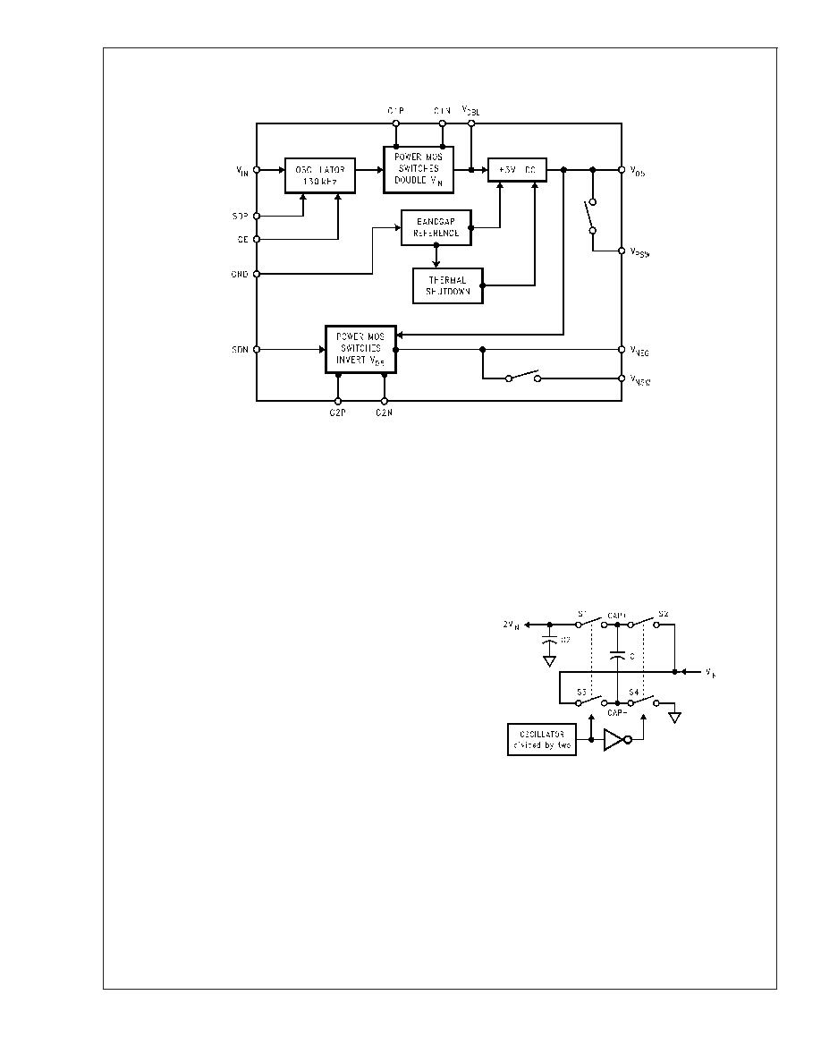
The LM2685 has three main functional blocks: a voltage
doubler, a low dropout (LDO) regulator, and a voltage in-
verter. Figure 1 shows the LM2685 functional block diagram.
VOLTAGE DOUBLER
The voltage doubler stage doubles the input voltage V
IN,
within the range of +2.85V to +5.4V. For V
IN above 5.4V, the
doubler shuts off and the input voltage is passed directly to
V
DBL via an internal power switch.
The doubler contains four large CMOS switches which are
switched in a sequence to double the input supply voltage.
Figure 2 illustrates the voltage conversion scheme. When S2
and S4 are closed, C1 charges to the supply voltage V
IN.
During this time interval, switches S1 and S3 are open. In the
next time interval, S2 and S4 are opened at the same time,
S1 and S3 are closed, the sum of the input voltage V
IN and
the voltage across C1 gives the 2V
In and the voltage across
C2 gives the 2V
IN at VDBL output. VDBL supplies the LDO
regulator. It is recommended not to load V
DBL when V05 has
a load of 50mA. For proper operation, the sum of V
DBL and
V
05 loads must not be more than 50mA.
The Schottky diode D1 is only needed for start-up. The
internal oscillator circuit uses the V
DBL and GND pins. The
voltage across them must be larger than 1.8V to ensure the
operation of the oscillator. During start-up, D1 is used to
charge up the voltage at V
DBL pin to start the oscillator; it
also protects the device from turning on its own parasitic
diode and potentially latching up. The diode should have
enough current carrying capability to change capacitor C3 at
start-up, as well as a low forward voltage to prevent the
internal parasitic diode from turning on. A Schottky diode like
1N5817 can be used for most applications. If the input ramp
is less than 10V/ms, a smaller schottky diode like
MBR0520LT1 can be used to reduce the circuit size.
+5 LDO REGULATOR
V
DBL is the input to an LDO regulator that regulates it to a +5
output voltage at V
05.VPSW is tied to V05 through a series
switch PSW. The LDO output capacitor (4.7F Tantalum)
may be tied to either V
05 or VPSW.
INVERTER
From the V
05 output, a 5V output is created at VNEG by
means of an inverting charge pump. This negative output is
unregulated, meaning that it’s output will droop as the load
current at V
NEG increases. The inverter contains four large
10110003
FIGURE 1. Functional Block Diagram
10110004
FIGURE 2. Voltage Doubler Principle
LM2685
www.national.com
6
发布紧急采购,3分钟左右您将得到回复。
相关PDF资料
LM2686MTCX/NOPB
SWITCHED CAPACITOR REGULATOR, 180 kHz SWITCHING FREQ-MAX, PDSO14
LM2787BPX/NOPB
0.01 A SWITCHED CAPACITOR REGULATOR, 450 kHz SWITCHING FREQ-MAX, PBGA8
LM2787TP/NOPB
0.01 A SWITCHED CAPACITOR REGULATOR, 450 kHz SWITCHING FREQ-MAX, PBGA8
LM2787BP/NOPB
0.01 A SWITCHED CAPACITOR REGULATOR, 450 kHz SWITCHING FREQ-MAX, PBGA8
LM285AH-1.2
1-OUTPUT TWO TERM VOLTAGE REFERENCE, 1.235 V, MBCY2
LM185AYH-1.2
1-OUTPUT TWO TERM VOLTAGE REFERENCE, 1.235 V, MBCY2
LM185AH-1.2
1-OUTPUT TWO TERM VOLTAGE REFERENCE, 1.235 V, MBCY2
LM285BEOA-2.5713
1-OUTPUT TWO TERM VOLTAGE REFERENCE, 2.5 V, PDSO8
相关代理商/技术参数
LM2686MTC
制造商:Texas Instruments 功能描述:VOLT CONVERTER SMD 2686 TSSOP14
LM2686MTC
制造商:Texas Instruments 功能描述:VOLT CONVERTER SMD 2686 TSSOP14
LM2686MTC/NOPB
功能描述:IC REG SWITCHED CAP DBL 14-TSSOP RoHS:是 类别:集成电路 (IC) >> PMIC - 稳压器 - DC DC 开关稳压器 系列:- 产品培训模块:Lead (SnPb) Finish for COTS
Obsolescence Mitigation Program 标准包装:1 系列:- 类型:降压(降压) 输出类型:固定 输出数:1 输出电压:3.3V 输入电压:4.5 V ~ 24 V PWM 型:- 频率 - 开关:- 电流 - 输出:125mA 同步整流器:无 工作温度:-40°C ~ 85°C 安装类型:表面贴装 封装/外壳:SOT-23-6 包装:Digi-Reel® 供应商设备封装:SOT-6 其它名称:MAX1836EUT33#TG16DKR
LM2686MTCX/NOPB
功能描述:IC REG SWITCHED CAP DBL 14-TSSOP RoHS:是 类别:集成电路 (IC) >> PMIC - 稳压器 - DC DC 开关稳压器 系列:- 产品培训模块:Lead (SnPb) Finish for COTS
Obsolescence Mitigation Program 标准包装:1 系列:- 类型:降压(降压) 输出类型:固定 输出数:1 输出电压:3.3V 输入电压:4.5 V ~ 24 V PWM 型:- 频率 - 开关:- 电流 - 输出:125mA 同步整流器:无 工作温度:-40°C ~ 85°C 安装类型:表面贴装 封装/外壳:SOT-23-6 包装:Digi-Reel® 供应商设备封装:SOT-6 其它名称:MAX1836EUT33#TG16DKR
LM2687LD
制造商:Texas Instruments 功能描述:
LM2687LD/NOPB
功能描述:IC REG SWITCHD CAP INV ADJ 8-LLP RoHS:是 类别:集成电路 (IC) >> PMIC - 稳压器 - DC DC 开关稳压器 系列:- 产品培训模块:Lead (SnPb) Finish for COTS
Obsolescence Mitigation Program 标准包装:1 系列:- 类型:降压(降压) 输出类型:固定 输出数:1 输出电压:3.3V 输入电压:4.5 V ~ 24 V PWM 型:- 频率 - 开关:- 电流 - 输出:125mA 同步整流器:无 工作温度:-40°C ~ 85°C 安装类型:表面贴装 封装/外壳:SOT-23-6 包装:Digi-Reel® 供应商设备封装:SOT-6 其它名称:MAX1836EUT33#TG16DKR
LM2687LDX
功能描述:电荷泵 RoHS:否 制造商:Maxim Integrated 功能:Inverting, Step Up 输出电压:- 1.5 V to - 5.5 V, 3 V to 11 V 输出电流:100 mA 电源电流:1 mA 最大工作温度:+ 70 C 封装 / 箱体:SOIC-8 Narrow 封装:Tube
LM2687LDX/NOPB
功能描述:电荷泵 RoHS:否 制造商:Maxim Integrated 功能:Inverting, Step Up 输出电压:- 1.5 V to - 5.5 V, 3 V to 11 V 输出电流:100 mA 电源电流:1 mA 最大工作温度:+ 70 C 封装 / 箱体:SOIC-8 Narrow 封装:Tube